The gate drive circuit of an IGBT is closely related to its static and dynamic characteristics. The positive bias voltage UGS, negative bias voltage -UGS and gate resistance RG of the gate circuit have different effects on the on-state voltage, switching time, switching loss, short-circuit capability and dv/dt of the IGBT. .
Some considerations for designing a driver circuit are as follows:
1) The length of the connection should be as small as possible to reduce the length of the connection between the pins of the IGBT module, especially the length of the gate leads. If you can't reduce its length, you can use a small magnetic ring or a small resistor in series with the gate. These two components should be as close as possible to the module gates to eliminate parasitic oscillations.
2) Carefully lay out the device as far as possible to be completely symmetrical. Connect the wires as long as possible and shorten as much as possible. Use as many strands as possible.
3) The bleeder resistor should be added with a drain resistance of 11kΩ between the gate and source of the IGBT.
4) Influence of positive bias voltage UGS When UGS increases, the turn-on time is shortened, and the turn-on loss is reduced. Although the increase of UGS is beneficial to reduce on-state voltage and turn-on loss, UGS cannot be increased arbitrarily. When it is increased to a certain extent, It has an adverse effect on the load short-circuit capability of the IGBT and dv/dt. This circuit uses UGS=15V.
5) Negative bias voltage - UGS influence Negative bias voltage is a very important gate drive condition, which directly affects the reliable operation of IGBT. Excessive dv/dt will generate a large displacement current, causing the voltage between the gate and the source to rise and exceed the gate threshold voltage of the IGBT, thus generating a large drain pulse surge current, which is too large. The drain surge current causes the IGBT to be uncontrollable. In order to avoid such false triggering of the IGBT, a reverse bias voltage can be applied to the gate. This circuit adds -UGS=-12V.
6) Influence of gate resistance The principle of gate resistance selection is that, in the case of low switching loss, a larger gate resistance should be selected, but when the gate resistance increases, the turn-on and turn-off time of the IGBT increases. In turn, the ON energy consumption EON and the shutdown energy consumption EOFF of each pulse are also increased, so the circuit is 51Ω.
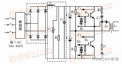
Power conversion part circuit diagram
7.62MM Power+ Signal Power Connector
power connector is used in power module system. It can select the matching power + signal connector according to the need. The feature is that the number of power and signal contacts and the matching sequence can be selected arbitrarily while keeping the connector size and contact core number unchanged.
Plug (male) / socket (female) can be installed at 90 or 180 degrees. It supports mixed or independent combination of signal and power. The quantity range of power and signal is (2-16) pin and (12-128) pin respectively
Product features
High temperature resistant, glass fiber reinforced and flame retardant polyester is used as insulation material
Copper gold composite conductor with high conductivity is used, and the contact area of the conductor is plated with gold
It adopts shrapnel contact, which has the characteristics of integration, small volume, large current carrying capacity, soft plug-in, blind plug-in, self guidance and high dynamic contact reliability. This series of products can be interchanged with FCI's powerblade series and Tyco's multi-beam series
There are three sizes of center distance of power contact: 5.08mm, 6.35mm and 7.62mm
The length of power hole / signal pin can be selected in two sizes. The power rated current is 45A and the signal rated current is 2.5A
7.62MM Power+ Signal Power Connector
ShenZhen Antenk Electronics Co,Ltd , https://www.antenkelec.com