The article on the electrical part of the physical layer was placed behind link initialization and training articles because this section involved related concepts such as Beacon Signal, LTSSM, and so on.
As mentioned earlier, since the articles in this series are mainly based on Gen2, the related contents of Gen3 will only be mentioned, but it will not be introduced in depth. If you are interested, you can read the Gen3's Spec yourself.
As mentioned in the article on link initialization and training, PCIe Spec states that PCIe devices that support the new standard must be backward compatible. That is, Gen2 devices must support 2.5GT/s and 5GT/s at the same time. However, it should be noted that Gen3 devices must support 2.5GT/s and 8GT/s while 5GT/s is optional.
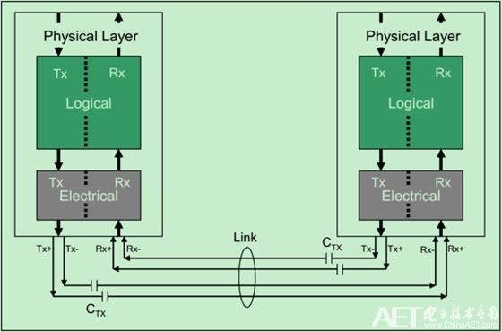
PCIe Spec stipulates that the PCIe device must be Short-Circuit Tolerant, which allows the PCIe card to support hot-swap functionality. In addition, since the PCIe bus is a high-speed differential bus, the transceiver ends are AC-Coupled. In general, a capacitor is placed on the link near the sender to filter out the DC signal, as shown in the following figure:
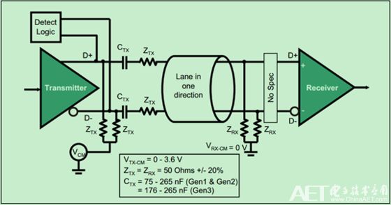
The detailed differential transceiver model is shown in the following figure:
Of course, if the PCIe device integrates the capacitance into the Silicon chip, it would be fine (though it wouldn't generally be the case, because the cost of integrating large capacitors inside the chip is very high). Another advantage of using AC coupling is that devices at both ends of the link can be allowed to use different power supplies and ground.
Note: Regarding the capacitor in the semiconductor and the ghost of a bunch of decoupling capacitors around the chip, I plan to find a time to write a separate article to talk in detail.
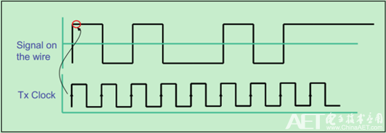
It should be noted that the PCIe bus uses an embedded clock, that is, only the data Lane, and no clock Lane (specifically described in detail in the previous article). In other words, taking Gen1 as an example, although the 2.5GT/s clock is 2.5GHz, from the data Lane, it seems that there is only 1.25GHz, as shown in the following figure:
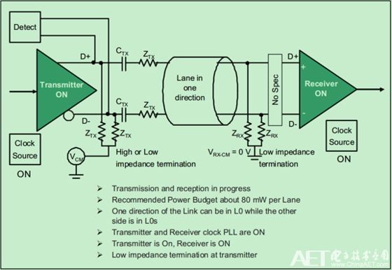
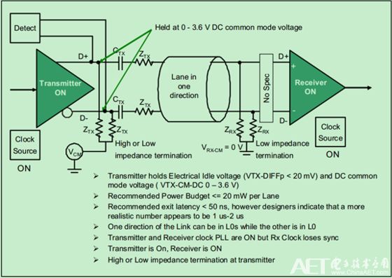
The link structure diagram (state diagram) in L0 mode is as follows:
The link structure diagram (state diagram) in L0s mode is as follows:
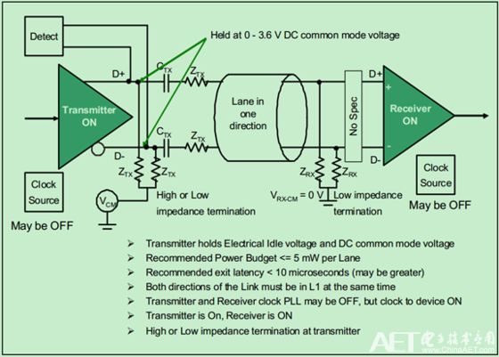
The L1 mode link structure diagram (state diagram) is as follows:
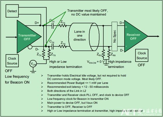
The L2 mode link structure diagram (state diagram) is as follows:
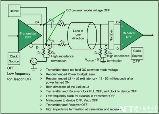
The L3 mode link structure diagram (state diagram) is as follows:
Kadena (KDA) is a hybrid blockchain network and smart contract platform that aims to unite public applications, private blockchains, and other interoperable chains in one place, driving traffic to the high-bandwidth computer at the heart of the Kadena public chain. Kadena`s mining algorithm is Blake2S, which supports ASIC mining.
Kadena is a blockchain network and smart contract token aiming to bring together both public applications and private blockchain.
The coin solves various problems that prevent blockchain adoption on a bigger scale. The protocol enables businesses and developers to make transactions and share information across many networks.
The Coin is actually on the grid to reduce users` experience in the network. Ethereum users experience a lot of network congestion which results in high gas fees.
A few changes have come into Kadena mining. A proof of work blockchain uses PACT to create smart contracts in the hidden gen. Therefore you need to know the following before mining Kadena. PACT is an intelligent contract language serving the needs of the blockchain community.
1.You Need an Excellent Mining Hardware
To mine efficiently, you will require suitable mining hardware. Kadena uses ASIC miners. But, unfortunately for Kadena miners, CPUs and GPUs are not usable. Furthermore, ASIC mining receives support from the Blake2S algorithm.
2.Make Sure You Have a Kadena Wallet Address
You will need a Kadena wallet address to receive and monitor your profit. F2pool also makes the distribution of the revenues to every user daily at 2KDA. The Kadena node wallet is a perfect wallet where you can receive your mined KDA. all you need to do is install it, click receive, and have a new wallet address.
You will need to configure your Asic Miner to a mining pool server for your hashrate and profit to be recorded and monitored.
3.Start Mining
After all the setting is done, your miner will be ready to work. Make sure you enter your wallet address and click on the go button to receive your revenue.
Kda Miner,Antminer Ka3 166Th,Bitmain Antminer Ka3 166Th,Antminer Bitmain Ka3
Shenzhen YLHM Technology Co., Ltd. , https://www.hkcryptominer.com