Abstract: A heart sound acquisition system based on FPGA is designed. The system includes a high-performance heart sound sensor, preprocessing circuit, A/D conversion circuit and serial communication circuit. The sensor converts the heart sound signal into an electrical signal, which is amplified and filtered by the pre-processing circuit, and then sent to the FPGA through the A/D conversion circuit. The FPGA transmits the data collected on-site to the PC in a timely and reliable manner. Experimental results show that the system can collect heart sound signals non-invasively, quickly and cheaply. Keywords: Heart sound signal; A/D; FPGA
At present, the diagnosis of cardiovascular diseases is mainly divided into two types: non-invasive diagnosis and invasive diagnosis. Among them, non-invasive diagnosis includes electrocardiogram, ambulatory electrocardiogram and phonocardiogram, echocardiogram and modern medical imaging technology [1]; invasive diagnosis mainly refers to arteriography technology, but it will bring complications. Very serious cardiovascular diseases cannot be diagnosed correctly by electrocardiogram, and early heart disease changes will cause changes in the components of the heart sound signal. The analysis of the heart sound components and murmurs through the electrocardiogram can make a correct diagnosis for early cardiovascular diseases. The heart sound signal is a very weak random signal, and noise is inevitably introduced during the acquisition process.
Wei Zhe et al. designed a heart sound signal acquisition and processing system based on a sound card [2]. This system makes full use of computer resources, but the computer itself has a lot of noise, and the signal-to-noise ratio of the collected signal is low. Tong Yinghua designed a heart sound and pulse signal acquisition system based on a single-chip microcomputer [3], but the single-chip microcomputer has the problem of low transmission rate. This paper designs a heart sound acquisition system based on FPGA. The heart sound signal-to-noise collected by this system is relatively high, which is suitable for follow-up research.
1 Overall scheme design of acquisition system
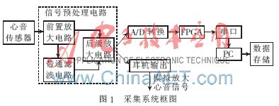
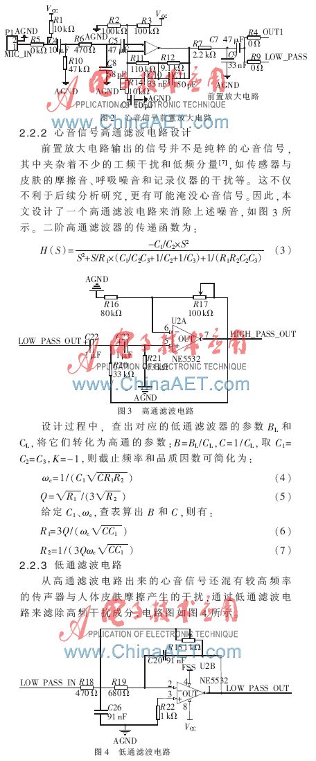
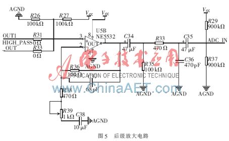
The block diagram of the acquisition system is shown in Figure 1. The system consists of a heart sound sensor, signal preprocessing circuit, A/D conversion circuit, and PC. Among them, the signal pre-processing circuit first amplifies the heart sound signal, then passes through a band-pass filter (consisting of a low-pass filter circuit and a high-pass filter circuit), and finally passes through the post-amplification circuit. The band-pass filter circuit can be controlled by a switch, and the output of the pre-amplifier can be controlled by the switch to skip the band-pass filter circuit and directly go to the post-amplifier circuit. Since the pre-stage signal only amplifies the heart sound signal to a few hundred millivolts, the signal is still very high. It is weak, so the heart sound signal is amplified to the +5 V range through the post-amplification circuit, and then output to the A/D conversion circuit. The A/D conversion circuit adopts the 8-bit, 32 MS/s analog-to-digital conversion single chip AD9280, the data after A/D conversion is directly transmitted to the FPGA, and the FPGA sends the data to the PC in real time through the serial port to realize the entire acquisition system.
2 Acquisition system implementation
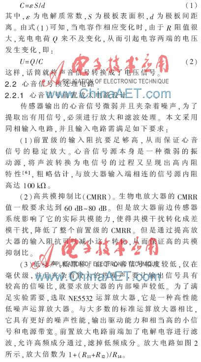
2.1 Research on Heart Sound Sensor
The heart sound sensor is an important part of the entire system, and its characteristics are critical to the quality of the collected signal. This paper designs a high-quality, low-cost heart sound sensor based on electret condenser microphone. The sensor has high sensitivity and strong anti-interference ability. In addition to extracting weak heart sound signals, it can also avoid interference from external noise as much as possible [4]. This sensor is composed of a miniature electret microphone and a stethoscope head. The stethoscope uses Oushi 130 K with a double-sided probe. Cut off the rubber tube of the stethoscope when making it, leaving about 10 cm. The sensor has a high sensitivity to heart sounds and almost no response to outside sounds [5]. After the diaphragm receives the sound wave, it vibrates correspondingly, and at the same time causes the distance between the plates to change. The capacitance calculation formula is:
2.3 A/D conversion circuit
The AD9280 is a single-chip, 8-bit analog-to-digital converter (ADC), powered by a single power supply, and built-in an on-chip sample-and-hold amplifier and reference voltage source. It uses a multi-stage differential pipeline architecture with a data rate of 32 MS/s, ensuring no missing codes in the entire working range. The inputs are designed to make the development of imaging and communication systems easier. The user can select various input ranges and offsets, and can drive the input in a single-ended or differential manner. The AD9280 has an on-chip programmable reference voltage source. An external reference voltage can also be used to meet the application's DC accuracy and temperature drift requirements. It adopts +2.7 V~+5.5 V power supply, which is very suitable for low-power operation in high-speed applications. The rated temperature range is -40℃~+85℃ industrial temperature range. The A/D conversion circuit is shown in Figure 6.

Nonwoven Fabric,Non Woven,Non Woven Material,Non Woven Geotextile Fabric
Longkou Libo Insulating Material Co.,Ltd. , https://www.sdliboinsulation.com