1. Resistance
When an alternating current flows through a conductor, the resistance it receives is called impedance (Impedance), which corresponds to Z and the unit is Ω.
The resistance at this time is different from the resistance encountered by the DC current. In addition to the resistance of the resistance, there are also the resistance problems of inductive reactance (XL) and capacitive reactance (XC).
In order to distinguish the resistance of direct current, the resistance encountered by alternating current is called impedance (Z).
Z=√ R2 +(XL -XC)2
2. Impedance (Z)
In recent years, with the improvement and application of IC integration, its signal transmission frequency and speed are getting higher and higher. Therefore, in the printed board wire, after the signal transmission (emission) reaches a certain value, it will be affected by the printed board wire itself. The impact of this, resulting in severe distortion or complete loss of the transmitted signal. This shows that the "thing" "circulated" by the PCB wire is not current, but the transmission of square wave signals or pulses in energy.
3. Characteristic impedance control (Z0)
The resistance encountered during transmission of the above-mentioned "signal" is also called "characteristic impedance", and its symbol is Z0.
Therefore, it is not enough to solve the problems of "on", "off" and "short circuit" on the PCB wires, and the characteristic impedance of the wires must be controlled. In other words, transmission lines for high-speed transmission and high-frequency signal transmission are much stricter in quality than transmission wires. It is no longer the "open/short circuit" test passed, or the gap or burr does not exceed 20% of the line width, it can be received. It must be required to determine the characteristic impedance value, and this impedance must also be controlled within the tolerance, otherwise, it will only be scrapped and not reworked.
2. Signal propagation and transmission line
1. Definition of signal transmission line
(1) According to the principle of electromagnetic waves, the shorter the wavelength (λ), the higher the frequency (f). The product of the two is the speed of light. That is, C = λ.f = 3×1010 cm/s
(2) Although any component has a high signal transmission frequency, after the PCB wire is transmitted, the original high transmission frequency will drop or the time will be delayed.
Therefore, the shorter the wire length, the better.
(3) It is advantageous to increase the PCB wiring density or shorten the wire size. However, with the acceleration of the component frequency or the shortening of the pulse period, the wire length approaches a certain range of the signal wavelength (speed). At this time, when the component is transmitted on the PCB wire, there will be obvious "distortion".
(4) IPC-2141 3.4.4 proposes: When the signal is transmitted in the wire, if the wire length is close to 1/7 of the signal wavelength, the wire at this time is regarded as a signal transmission line.
(5) Examples:
The signal transmission frequency (f) of a certain component is 10MHZ, and the length of the wire on the PCB is 50cm. Should characteristic impedance control be considered?
Solution: C = λ.f ï¼3×1010 cm/s
λ=C/f=(3 ×1010 cm/s)/(1 ×107 /s)=3000cm
Wire length/signal wavelength = 50/3000 = 1/60
Because: 1/60<1/7, this wire is an ordinary wire, so there is no need to consider the characteristic impedance.
In electromagnetic wave theory, Maxwell's formula tells us: The propagation speed VS of sine wave signal in the medium is proportional to the speed of light C, and inversely proportional to the dielectric constant of the transmission medium.
VS ï¼C/√εr
When εr =1, the signal transmission reaches the propagation speed of light, that is, 3×1010 cm/s.
2. Transmission rate and dielectric constant
Signal transmission speed of different plates under 30MHZ
Dielectric material Tg (°C) Dielectric constant signal transmission speed (m/µs)
Vacuum/ 1.0 300.00
PTFE/2.2 202.26
Thermosetting polypropyl ether 210 2.5 189.74
Cyanate resin 225 3.0 173.21
PTFE resin + E glass cloth/ 2.6 186.25
Cyanate resin + glass cloth 225 3.7 155.96
Polyimide + glass cloth 230 4.5 141.42
Quartz/ 3.9 151.98
Epoxy glass cloth 130±5 4.7 138.38
Aluminum/ 9.0 100.00
It can be seen from the above table that as the dielectric constant (εr) increases, the transmission speed of the signal in the dielectric material decreases. To obtain a high signal transmission speed, a high characteristic impedance value is required; for a high characteristic impedance, a low dielectric constant (εr) material must be selected; the dielectric constant (εr) of PTFE (Teflon) is the smallest, and the transmission The fastest.
FR-4 board is composed of epoxy resin and E-grade glass cloth, with a dielectric constant (εr) of 4.7. The signal transmission speed is 138m/μs. Changing the resin system can easily change the dielectric constant (εr).
3. Reasons for characteristic impedance control
1. Reason one
When the electronic equipment (computer, communication machine) is operated, the signal sent by the driver component (Driver) will reach the receiver component (Receiver) through the PCB transmission line. When the signal is transmitted in the signal line of the printed board, its characteristic impedance value Z0 must match the "electronic impedance" of the head and tail components, so that the "energy" in the signal can be completely transmitted.
2. Reason two
Once the printed board is of poor quality and Z0 exceeds the tolerance, the transmitted signal will have problems such as reflection, dispersion, attenuation or delay. In severe cases, the signal will be transmitted incorrectly and the machine will crash.
3. Reason three
Strictly select the board and control the production process, so that the Z0 on the multilayer board can meet the specifications required by the customer. The higher the electronic impedance of the component, the faster its transmission speed, so the Z0 of the PCB must be increased accordingly to meet the requirements of matching components. Z0 qualified multi-layer boards can be regarded as qualified products required for high-speed or high-frequency signals.
Fourth, the relationship between characteristic impedance ZO and plate and process
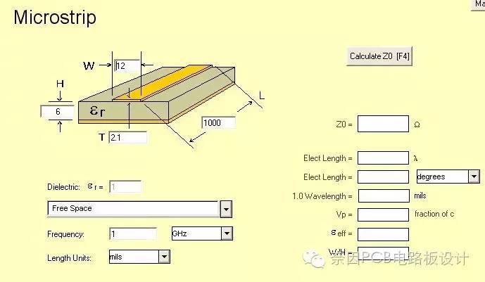
The characteristic impedance Z0 calculation formula of the microstrip line structure: Z0 = 87/r +1.41 ln5.98H / (0.8W+T)
Among them: εr-dielectric constant H-dielectric thickness W-wire width T-wire thickness
The lower the εr of the board, the easier it is to increase the Z0 value of the PCB circuit and match the output impedance value of the high-speed component.
1. The characteristic impedance Z0 is inversely proportional to the εr of the plate
Z0 increases as the thickness of the medium increases. Therefore, for high-frequency circuits with strict Z0, strict requirements are imposed on the error of the dielectric thickness of the copper clad substrate. Generally, the thickness of the media must not vary more than 10%.
2. The influence of dielectric thickness on characteristic impedance Z0
With the increase of trace density, the increase of dielectric thickness will cause the increase of electromagnetic interference. Therefore, for signal transmission lines of high-frequency lines and high-speed digital lines, with the increase of conductor wiring density, the thickness of the medium should be reduced to eliminate or reduce the noise or crosstalk caused by electromagnetic interference, or to greatly reduce εr. εr substrate.
According to the characteristic impedance Z0 calculation formula of the microstrip line structure: Z0 = 87/r +1.41 ln5.98H / (0.8W+T)
The thickness of the copper foil (T) is an important factor that affects Z0. The greater the thickness of the wire, the smaller the Z0. But its range of change is relatively small.
3. The influence of copper foil thickness on characteristic impedance Z0
The thinner the thickness of the copper foil, the higher the Z0 value can be obtained, but the thickness change does not contribute much to Z0.
The contribution of thin copper foil to Z0 is not as accurate as the contribution of thin copper foil to the manufacture of fine wires to improve or control Z0.
According to the formula:
Z0 = 87/r +1.41 ln5.98H / (0.8W+T)
The smaller the line width W, the larger Z0; reducing the wire width can increase the characteristic impedance.
The line width change has a much more obvious effect on Z0 than the line thickness change.
4. The influence of wire width on characteristic impedance Z0
Z0 increases rapidly as the line width W becomes narrower. Therefore, to control Z0, the line width must be strictly controlled. At present, the signal transmission line width W of most high-frequency circuits and high-speed digital circuits is 0.10 or 0.13mm. Traditionally, the line width control deviation is ±20%. The PCB wires of conventional electronic products that are not transmission lines (wire length <1/7 of the signal wavelength) can meet the requirements, but for signal transmission lines with Z0 control, the PCB wire width deviation is ±20%, which can no longer meet the requirements. Because at this time the Z0 error has exceeded ±10%.
Examples are as follows:
The width of a PCB microstrip line is 100μm, the line thickness is 20μm, and the dielectric thickness is 100μm. Assuming that the copper thickness of the finished PCB is uniform, ask if the line width changes by ±20%, can Z0 be within ±10%?
Solution: According to the formula
Z0 = 87/r +1.41 ln5.98H / (0.8W+T)
Substitution: line width W0 = 100μm, W1 = 80μm, W2 = 120μm, line thickness T = 20μm, dielectric thickness H = 100μm, then: Z01 /Z02 =1.20
Therefore, Z0 is just ±10%, which cannot reach <±10%.
To achieve the characteristic impedance Z0 <±10%, the wire width deviation must be further reduced, and it must be far less than ±20%.
Similarly, to control Z0 ≤5%, the wire width tolerance must be controlled ≤±10%.
Therefore, it is not difficult for us to understand why PTFE PCBs and some FR-4 PCBs require a line width of ±0.02mm, and the reason is to control the characteristic impedance Z0 value.
Five, characteristic impedance control printed board process control
1. Film production management and inspection
Constant temperature and humidity room (21±2°C, 55 ± 5%), dustproof; line width process compensation.
2. Jigsaw design
The edge of the jigsaw panel should not be too narrow, the plating layer is uniform, and the electroplating adds false cathodes to disperse the current;
Design a coupon for the Z0 edge test on the jigsaw board.
3. Etching
Strict process parameters, reduce side corrosion, and conduct first inspection;
Reduce residual copper, copper slag, and copper scrap at the edge of the wire;
Check the line width and control it within the required range (± 10% or ± 0.02mm).
4. AOI inspection
The inner layer board must find wire gaps and protrusions. For 2GHZ high-speed signals, even 0.05mm gaps must be scrapped; controlling the inner layer line width and defects is the key.
5. Laminating
Vacuum laminator, reduce the pressure to reduce the flow of glue, try to keep as much resin as possible, because the resin affects the εr, the resin is stored more, and the εr will be lower. Control the tolerance of laminate thickness. Because the thickness of the plate is not uniform, it indicates that the thickness of the medium changes, which will affect Z0.
6. Choose the base material
Strictly cut the material according to the plate model required by the customer. The model is wrong, the εr is wrong, the board thickness is wrong, the PCB manufacturing process is all right, and the same is scrapped. Because Z0 is greatly affected by εr.
7. Solder mask
The solder mask on the board surface will reduce the Z0 value of the signal line by 1 to 3Ω. Theoretically, the solder mask thickness should not be too thick, but in fact the effect is not very large. The surface of the copper wire is in contact with air (εr = 1), so the measured Z0 value is higher. However, the Z0 value measured after the solder mask will drop by 1 to 3Ω, because the εr of the solder mask is 4.0, which is much higher than that of air.
8. Water absorption
The finished multi-layer board should avoid water absorption as much as possible, because the εr of water = 75, which will bring a great drop and unstable effect to Z0.
Six, summary
The characteristic impedance Z0 of the multi-layer board signal transmission line currently requires a control range of: 50Ω±10%, 75Ω±10%, or 28Ω±10%.
To control the scope of change, four factors must be considered:
(1) Signal line width W;
(2) Signal wire thickness T;
(3) The thickness of the dielectric layer H;
(4) Dielectric constant εr.
The biggest influence is the dielectric thickness, followed by the dielectric constant, the wire width, and the smallest is the wire thickness. After the substrate is selected, the change of εr is very small, the change of H is also small, T is easier to control, but it is difficult to control the line width W to ±10%, and the line width problems include pinholes, notches, dents, etc. on the wire problem. In a sense, the most effective and important way to control Z0 is to control and adjust the line width.
Best Budget I7 Laptop is everyone eager to. Laptop Intel Core i7 is the No. 1 processor clients choose when they are searching for a performance Gaming Laptop,cause it`s of excellent powering, bigger Solid State Drive, usually 512GB based, full HD 16:9 aspect ratio slimmer display bezels, bigger battery-12000mAh-no need to worry lack of power, fingerprint reader, backlight keyboard, etc. What is intel Core I7 Laptop Price? Usually 300-400usd. You can get Intel i7 11th Generation Laptop, Intel i7 10th Generation Laptop, Intel I5 11th Generation Laptop, Laptop I3 11th Generation,etc. 15.6 or 14 inch all available for i7 processor.
Cooperating with us, you just need to share all your requirements details, like size, cpu, ram, rom, battery, fingerprint, backlight, enter button numbers, SSD+HDD or only SSD ok, if need oem service, if need logo position, special apps preinstall if need, etc. Can provide matched and value feedback in 1-2 working days.
The reason why clients choose us is that just half of DOA than others, longer warranty time, smaller MOQ, fast delivery, competitive cost, good after-sale service, etc.
Laptop Intel Core I7,Intel Core I7 Laptop Price,Best Budget I7 Laptop,Intel I7 11th Generation Laptop,Intel I7 10th Generation Laptop
Henan Shuyi Electronics Co., Ltd. , https://www.shuyilaptop.com