Due to the switching characteristics of the switching power supply, it is easy for the switching power supply to cause great electromagnetic compatibility interference. As a power supply engineer, an electromagnetic compatibility engineer, or a PCB layout engineer, it is necessary to understand the cause of the electromagnetic compatibility problem, especially the layout. Engineers need to understand how to avoid the expansion of dirty spots. This article mainly introduces the main points of power PCB design.
29 basic relationships between layout and PCB
1. Several basic principles: any wire is impedance; the current always selects the path with the lowest impedance; the radiation intensity is related to the current, frequency, and loop area; common mode interference and large dv/dt signals are related to the mutual capacitance of the ground. The principles of reducing EMI and enhancing immunity are similar.
2. The layout should be partitioned according to power supply, analog, high-speed digital and various function blocks.
3, try to reduce the large di / dt loop area, reduce the length of the large dv / dt signal line (or area, width should not be too wide, the increase in the trace area to increase the distributed capacitance, the general approach is: the width of the trace Try to be as big as possible, but remove the excess) and try to take a straight line and lower its hidden area to reduce the radiation.
4. Inductive crosstalk is mainly caused by large di/dt loops (loop antennas). The induced intensity is directly proportional to the mutual inductance. Therefore, it is more important to reduce the mutual inductance of these signals (the main way is to reduce the loop area and increase the distance). Sexual crosstalk is mainly generated by large dv/dt signals. The induced intensity is proportional to the mutual capacitance. All the reductions and the mutual capacitance of these signals (the main way is to reduce the coupling effective area, increase the distance, and reduce the mutual capacitance with the increase of the distance). Faster) is more critical.
5, try to use the principle of loop cancellation to route, further reduce the area of ​​the large di / dt loop, as shown in Figure 1 (similar to twisted pair
Improve the anti-interference ability and increase the transmission distance by using the loop cancellation principle):
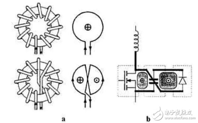
Figure 1. Loop cancellation (freewheeling of the boost circuit)
640mm*1600mm LED Poster Display
P3 LED Poster,LED Poster Price,Digital LED Poster,Transparent LED Poster
ShenZhen UHLED Technology Co., LTD. , https://www.uhled.com