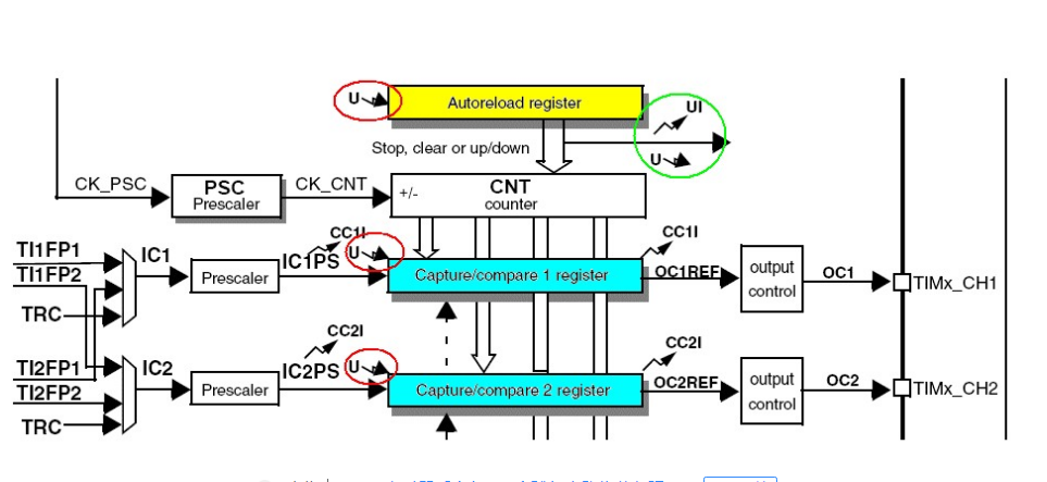
This STM32 MCU is the STM32F103 series.
The STM32 ADC has DMA function, which is undoubtedly the most used by us! However, if we want to periodically sample a signal (such as a pulse signal) (that is, every second, say 2ms), there are three ways:

1. Use the timer interrupt to perform ADC conversion at regular intervals, so you must read the ADC data register every time, which is a waste of time!
2. Set the ADC to continuous conversion mode, and the corresponding DMA channel turns on the loop mode, so the ADC has been collecting data and then transferring data to the memory through DMA. But if you do this, you have to add a timed interrupt to periodically read the data in memory!
3. Use the ADC's timer to trigger the ADC conversion function, and then use DMA to carry the data! In this way, as long as the trigger interval of the timer is set, the function of the ADC timing sampling conversion can be realized, and then the DMA conversion completion flag can be detected in the infinite loop of the program, and then the data can be read, or the DMA conversion completion interrupt can be enabled. This will generate an interrupt each time the conversion is completed. I am using the second method. Below the code: I use a single channel here
/ / Timer initialization
voidTIM2_ConfiguraTIon(void)
{
TIM_TImeBaseInitTypeDefTIM_TimeBaseStructure;
TIM_OCInitTypeDefTIM_OCInitStructure;
RCC_APB1PeriphClockCmd(RCC_APB1Periph_TIM2, ENABLE);
TIM_TimeBaseStructure.TIM_Period=1999;//Set the period of 2ms TIM2 comparison
TIM_TimeBaseStructure.TIM_Prescaler=71;//The system clocked at 72M, where the frequency is 71, which is equivalent to 1000K timer 2 clock.
TIM_TimeBaseStructure.TIM_ClockDivision=0x0;
TIM_TimeBaseStructure.TIM_CounterMode=TIM_CounterMode_Up;
TIM_TimeBaseInit(TIM2,&TIM_TimeBaseStructure);
TIM_OCInitStructure.TIM_OCMode=TIM_OCMode_PWM1;//Detailed below
TIM_OCInitStructure.TIM_OutputState=TIM_OutputState_Enable;//TIM_OutputState_Disable;
TIM_OCInitStructure.TIM_Pulse=1000;
TIM_OCInitStructure.TIM_OCPolarity=TIM_OCPolarity_Low;//If PWM1 is Low, PWM2 is High
TIM_OC2Init(TIM2,&TIM_OCInitStructure);
//TIM_InternalClockConfig(TIM2);
//TIM_OC2PreloadConfig(TIM2, TIM_OCPreload_Enable);
//TIM_UpdateDisableConfig(TIM2, DISABLE);
}
//ADC_DMA initial configuration
voidADC_DMA_Config(void)
{
DMA_InitTypeDefDMA_InitStructure;//Note: ADC is a 12-bit analog-to-digital converter, only the lower 12 bits of ADCConvertedValue are valid.
RCC_AHBPeriphClockCmd (RCC_AHBPeriph_DMA1, ENABLE); / / enable DMA clock
DMA_DeInit(DMA1_Channel1);//Open the first channel of DMA1
DMA_InitStructure.DMA_PeripheralBaseAddr=ADC1_DR_Address;//DMA corresponding peripheral base address
DMA_InitStructure.DMA_MemoryBaseAddr=(uint32_t)&ADCConvertedValue;//memory storage base address
DMA_InitStructure.DMA_DIR=DMA_DIR_PeripheralSRC;//DMA conversion mode is SRC mode, moved from peripheral to memory
DMA_InitStructure.DMA_BufferSize=1;//DMA cache size, 1
DMA_InitStructure.DMA_PeripheralInc=DMA_PeripheralInc_Disable;// After receiving data once, the device address is forbidden to move backward
DMA_InitStructure.DMA_MemoryInc=DMA_MemoryInc_Disable;//The target memory address is moved backward after receiving the data once.
DMA_InitStructure.DMA_PeripheralDataSize=DMA_PeripheralDataSize_HalfWord;//Define peripheral data width is 16 bits
DMA_InitStructure.DMA_MemoryDataSize=DMA_MemoryDataSize_HalfWord;//DMA moves data size, HalfWord is 16 bits
DMA_InitStructure.DMA_Mode=DMA_Mode_Circular;//cyclic conversion mode
DMA_InitStructure.DMA_Priority=DMA_Priority_High;//DMA priority is high
DMA_InitStructure.DMA_M2M=DMA_M2M_Disable;//M2M mode disabled
DMA_Init(DMA1_Channel1, &DMA_InitStructure);
DMA_ITConfig (DMA1_Channel1, DMA_IT_TC, ENABLE); / / enable transmission completion interrupt
}
//ADC initialization
voidPulseSenosrInit(void)
{
//When the external trigger signal is selected as the ADC rule or injection conversion, only its rising edge can initiate the conversion.
ADC_InitTypeDefADC_InitStructure;
ADC_GPIO_Configuration();//IO port configuration
TIM2_Configuration();//Timer configuration
ADC_DMA_Config();//ADC_DMA configuration
ADC_InitStructure.ADC_Mode=ADC_Mode_Independent;//Independent conversion mode ADC_DUALMOD[3:0]=0000;
ADC_InitStructure.ADC_ScanConvMode=DISABLE;// Turn off scan mode because there is only one channel
ADC_InitStructure.ADC_ContinuousConvMode=DISABLE;// Turn off continuous conversion mode, otherwise just trigger once,
//The subsequent conversion will never stop (unless CONT is cleared to 0), so the ADC after the first time is not triggered by TIM2_CC2.
ADC_InitStructure.ADC_ExternalTrigConv=ADC_ExternalTrigConv_T2_CC2;//Software Conversion Mode
ADC_InitStructure.ADC_DataAlign=ADC_DataAlign_Right;//Alignment mode, ADC is 12 bits, right alignment ADC_ALIGN=0;
ADC_InitStructure.ADC_NbrOfChannel=1;//Open channel number, 1 ADC_SQR1[23:20]=0000;
//ADC_SQR1[23:20] sets the number of channels to choose from.
ADC_Init(ADC1,&ADC_InitStructure);
/ / RCC_ADCCLKConfig (RCC_PCLK2_Div6); / / configuration clock (12MHz), should also be configured in the RCC APB2 = AHB clock 72MHz
ADC_RegularChannelConfig(ADC1, ADC_Channel_2, 1, ADC_SampleTime_1Cycles5);
//ADC_SMPR2ADC_SMPR1 sets the sampling time for each channel
//ADC_SQR1[19:0]DC_SQR1[29:0]DC_SQR3[29:0]Set the conversion order of the corresponding channel for multi-channel sampling
/ / ADC channel group, the third channel sampling sequence 1, conversion time
ADC_ExternalTrigConvCmd(ADC1,ENABLE);//Set the external trigger mode enable (this "external" is actually only the phase / / for the outside of the ADC module,
ADC_DMACmd (ADC1, ENABLE);
ADC_Cmd(ADC1,ENABLE);//ADC command, enable ADC_ADON=1
ADC_ResetCalibration(ADC1);//Recalibration
While(ADC_GetResetCalibrationStatus(ADC1));//waiting to recalibrate
ADC_StartCalibration(ADC1);//Start calibration ADC_RSTCAL=1; Initialize calibration register
While(ADC_GetCalibrationStatus(ADC1));//waiting for calibration to complete ADC_CAL=0;
//ADC_SoftwareStartConvCmd(ADC1,ENABLE);//Continuous conversion starts, and the ADC continuously updates the RAM area by DMA.
/ / ADC_SWSTART = start rule conversion remember software trigger is also an external event to set ADC_EXTTRIG = 1
//////It’s actually inside STM32)
TIM_Cmd (TIM2, ENABLE); / / last open timer enable
DMA_Cmd (DMA1_Channel1, ENABLE); / / enable DMA
}
/ / interrupt handler
voidDMA1_Channel1_IRQHandler(void)
{
If(DMA_GetITStatus(DMA1_IT_TC1)!=RESET){
/ / Own interrupt processing code but remember that the program is not too complicated, it is best not to exceed the interruption time
DMA_ClearITPendingBit(DMA1_IT_TC1);
}
}
/ / interrupt configuration
NVIC_InitTypeDefNVIC_InitStructure;
NVIC_PriorityGroupConfig(NVIC_PriorityGroup_1);
NVIC_InitStructure.NVIC_IRQChannel=DMA1_Channel1_IRQn;
NVIC_InitStructure.NVIC_IRQChannelPreemptionPriority=0;
NVIC_InitStructure.NVIC_IRQChannelSubPriority=0;
NVIC_InitStructure.NVIC_IRQChannelCmd=ENABLE;
NVIC_Init(&NVIC_InitStructure);
voidADC_GPIO_Configuration(void)//ADC configuration function
{
GPIO_InitTypeDefGPIO_InitStructure;
RCC_APB2PeriphClockCmd(RCC_APB2Periph_ADC1|RCC_APB2Periph_GPIOA, ENABLE); //Enable ADC and GPIOA clock
GPIO_InitStructure.GPIO_Pin=GPIO_Pin_2;//pin 2
GPIO_InitStructure.GPIO_Mode=GPIO_Mode_AIN;//analog input mode
GPIO_Init(GPIOA,&GPIO_InitStructure);//GPIO group
}
Shenzhen Enershare Technology Co.,Ltd , https://www.enersharepower.com