1. When the component package is made, there is no electrical connection pad. What is the definition of the pin number?
A: When placing a pad, you should select Mechanical Figure:

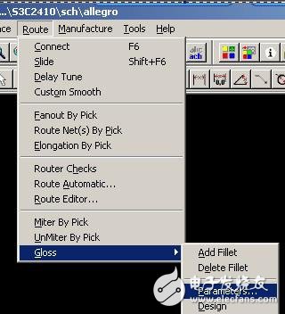
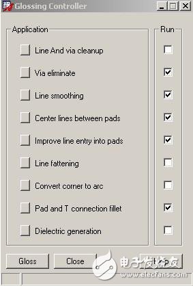
2. In Allegro, how to add tears?
Answer: To open all the routing layers first, run the command route-"gloss-"parameters. Dialog box appears, click on pad and T connecTIon fillet, then click on the left square, click on circular pads, pins, vias, T connecTIons./OK/GLOSS.
Note: Whether you add teardrops or teardrops, be sure to turn on all the trace layers first. Otherwise, the trace layers that are not turned on will not be executed.
Pictured:
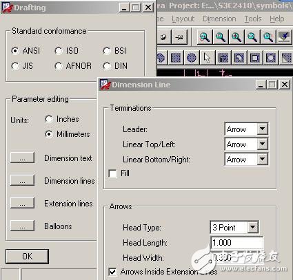
3, (1) The dimension is best marked with a 1x0.3 size arrow, set to:
Arrow -》 3point
Head length:1.0
Head width: 0.3
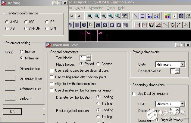
(2) The dimension text is set to: Text block: 3
Arrow settings as shown:
Text size settings as shown:
4, Q: What shortcut keys to switch Allegro layer?
Switch between "-" and "+"!
5, how to achieve the COPY wireframe? Is there a way to COPY the Package Geometry -> silkscreen_top line to Package Geometry - Assembly_top when doing component packaging?
Select copy, point in the silkscreen wireframe, drag the copied wireframe away from the original wireframe, and then change to the assembly, move the assembly wireframe mov back to the original wireframe position, and complete the copy.
6. What is the difference between Display_Top, Assemble_Top, and Silkscreen_Top?
7, when the component package, the pad can not be replaced? Not delete and put again. For example: smd91x17.pad is replaced by smd91x16b.pad.
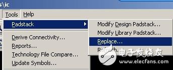
→
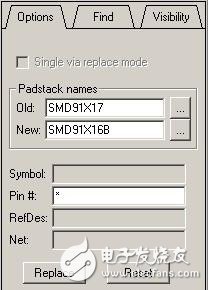
Then click on Replace.
8. How to set the three types of differential line, snake line, and other long line? How is it painted?
9. Blind vias connect several internal PCBs to the surface PCB without penetrating the entire board. Buried vias connect only the internal PCB.
10. Can I just close the copper and keep the etch?
can! Click the Uers Preference... option under the SETUP menu and select the right SHAPE option to hook no_shape_filt.
11, how to change the number of good pad number?
Open the Pin_Number layer and use Edit - Text to modify it.
12. How to rotate the PCB board 90 degrees in allegro?
Select the MOVE command (Point select User Pick under OpTIons, hook everything you want in Find)
Right-click to select Temp Group
Select the entire board (you can also select one or more parts you need)
Right-click to select Complete
Click a bit as User Pick
Right-click to select Rotate
You can rotate it
13. How do I set different networks to have different colors in Allegro?
Hilight --- In the optoons next to the control bar, select the color, in the Finder, check the net, enter the name of the network to be highlighted, or point the network fly directly.
14. Renumber the repaired schematics
Tools – Annotate ...
15. How to divide an element into two parts? How to divide part1 and part2 when Capture draws a component library?
Click on the Next part below the View menu.
There is a package type option under the new library.
Homogeneous: the same kind.
Heterogeneous: heterogeneous, heterogeneous.
If you want to make two identical PARTs, select the first one and change the parts per PKG. to 2 at the same time. If you want to make two different PARTs, select the second item and change the parts per PKG. to 2 at the same time.
16. The device drawn in the schematic is now modified in the library. How can I update it in the schematic (without deleting the original device and relocating it)?
17, in allegro, how to lock the components?
Click to select the component to be locked.
18, allegro, in the case of the network fly off the network, moving components, can display the network fly?
As long as these two are not ticked, the fly line was originally displayed, and then the fly line can be displayed when moving.
10.1 Inch Laptop,win10 Laptops,win11 Laptops
Jingjiang Gisen Technology Co.,Ltd , https://www.gisentech.com